PCB tools
The experimentation room provides basic tools to assemble electronic components on a prefabricated PCB.
Workflow
stateDiagram
    direction LR
    c1: PCB Design (KiCad, Altium)
    c2: Order PCB
    c3: Order Components
    r1: Manufactured PCB
    r2: Print paste on the PCB
    r3: Ordered components
    r4: Pick and place components
    r5: Perform reflow soldering in oven
    state Computer {
        c1 --> c2
        c1 --> c3
    }

    Computer --> Room
    Room: Experimentation room
    state Room {
        r1 --> r2
        r2 --> r4
        r3 --> r4
        r4 --> r5
    }
Manual solder paste printer
This machine is used to apply soldering paste on the ordered PCB. It is important to also order a PCB stencil along with the PCB manufacturing.
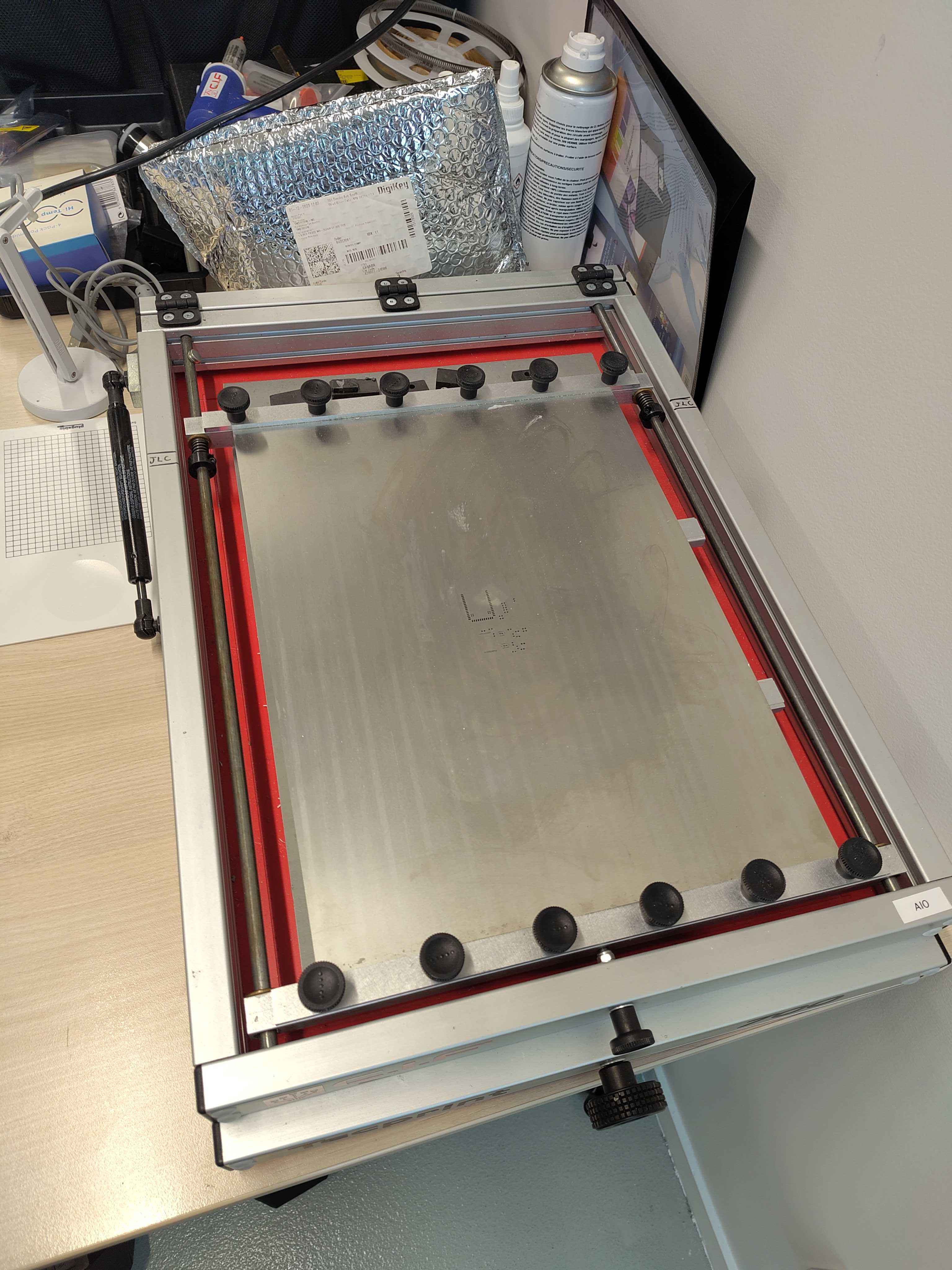
Once the paste is applied, use the soldering microscope to verify it's correctly applied: no missing pads, not too much paste on tiny pads, etc
Pick and place
The pick and place is used to place all components on the PCB. We recommend to carefully prepare and sort the components as follows: - label the components bags with the labels used to name the components on the PCB. This saves a lot of time and avoids potential mistakes during the process - display the board layout on a laptop beside the pick and place
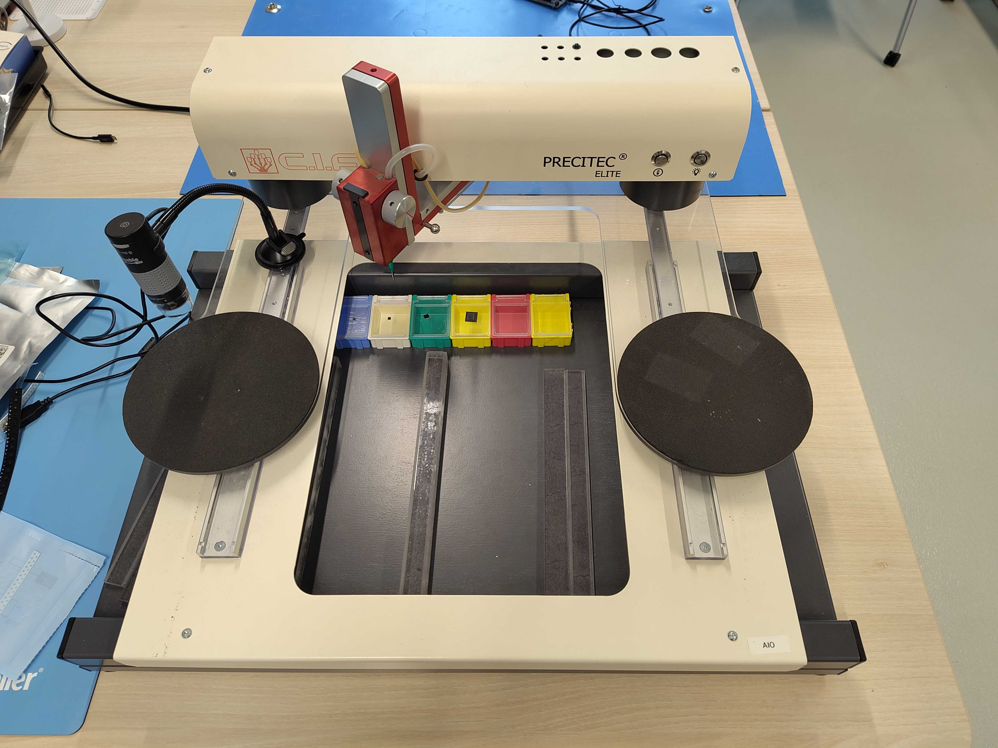
Note
Unless you have very good eyes it's better to avoid too small components in the PCB design, like SMD 0402. Some BGA components with tiny pads might also be challenging to assemble with this machine.
Once all components are placed, check again the result with the soldering microscope. Things to check are correct placement and orientation of the components
Reflow oven
This is the last step of the assembly: reflow soldering.
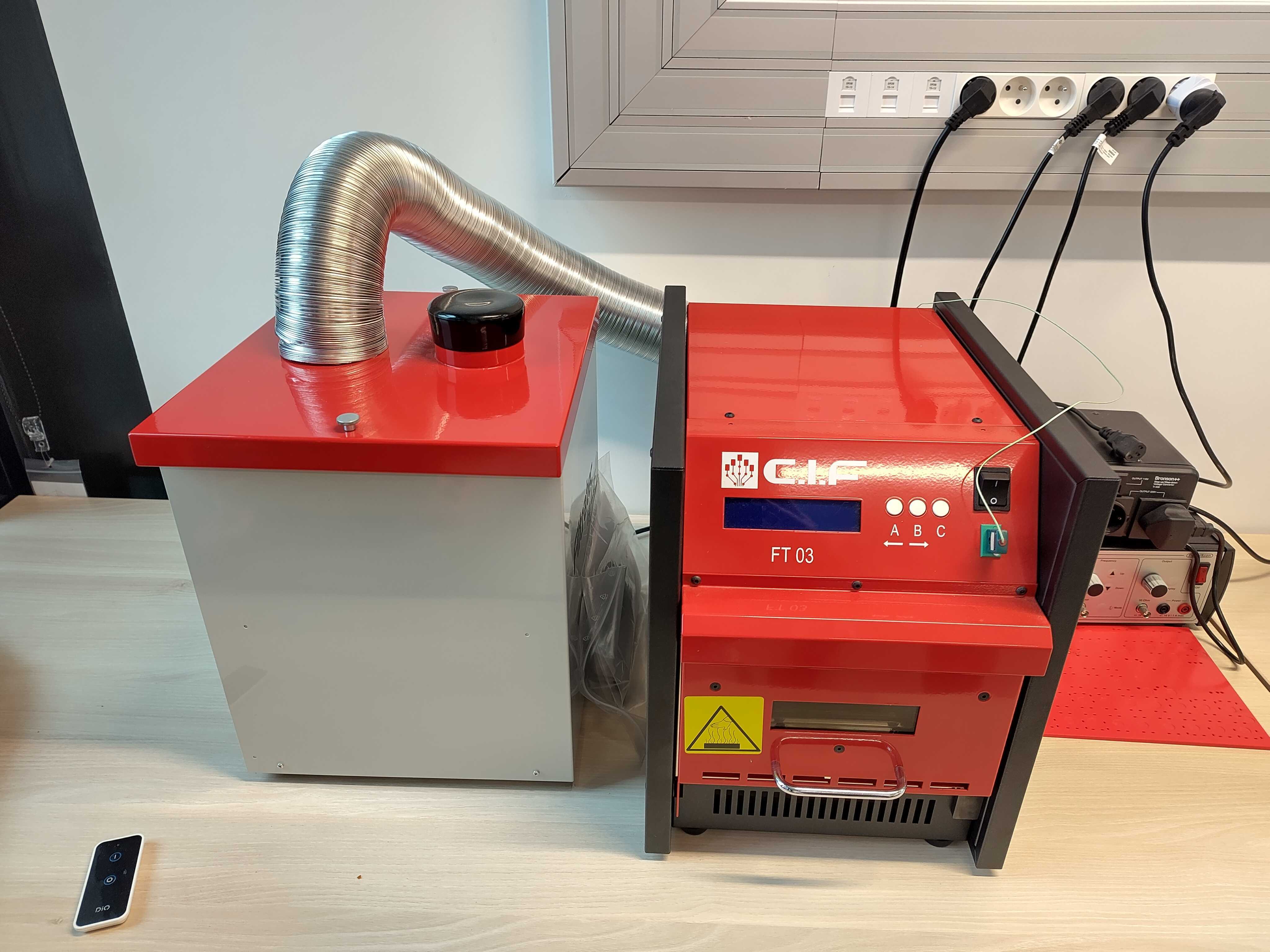
Usage
-
Place the PCB in the oven
-
Power on the fume extractor using the remote control
-
Power on the oven, press C